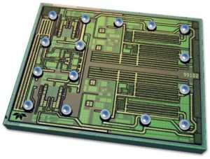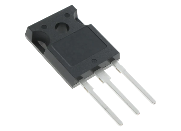
The transistors (right) are both enhancement-mode, top-side-cooled GaN-on-silicon hemts.
“The parts go through NASA Level 1 screening flow and can be brought up to full Level 1 conformance with extra qualification testing if desired,” according to Teledyne.
“Our GaN hemt product family has been very popular with customers, and we have had many requests for catalogue versions with standard space screening,” added Teledyne business development v-p Mont Taylor.
The devices are:
- TDG650E601TSP with 900V transient drain-to-source maximum
- TDG650E602TSP with 750V transient drain-to-source maximum
Each is available with EAR99 or European sourcing.
They are single wafer lot traceable, work over -55 to +125°C, and are designed to have low inductance and low thermal resistance.
 At the same time, it announced a 100V gate driver for 20MHz power supplies, the TD99102 (left).
Made on a silicon-on-insulator process, it will offer “the performance of GaAs with the economy and integration of conventional CMOS”, said Teledyne, “It features 100krad(Si) total ionising dose and single-event latch-up immunity. Outputs are capable of switching transitions in the sub-nanosecond range.”
The bumped flip-chip die has dead-time control, and offers 2A peak source current and 4A peak sink current.
Applications for the transistors and driver are foreseen in dc-dc and ac-dc converters, point-of-load modules and motor drives in low-Earth and medium-Earth orbits.


