The node-to-node improvement is diminishing even as costs continue to increase due to integration complexity.
On the design side, there is a trend to create more domain specific accelerators for each function like neural processing, graphics, video, etc. and a much stronger focus on hardware-software co-optimization to gain more at the system level.
There is also a drive to identify specific technologies to address system bottlenecks like the memory wall (how to get data at high bandwidth, with sufficient speed and low enough power to feed the logic cores), power wall (how to efficiently handle power delivery and thermal dissipation) or datacom bottlenecks (how to ensure wired, photonics and wireless infrastructure can handle the exponentially increasing data traffic) instead of relying on off-the-shelf generic technologies.
There is a drive to identify specific technologies to address system bottlenecks like the memory wall, power wall or datacom bottlenecks instead of relying on off-the-shelf generic technologies.
There are examples in high-performance compute space like AMD’s V-cache technology where 3D integration is used to bring extra SRAM memory closer to the CPU.
Another example is the use of a silicon interposer bridge to connect two CPU die in the Apple M1 Ultra system-on-chip (SoC).
There is also a strong push to co-package the electronic and photonic ICs leveraging different 3D and 2.5D technologies to reduce parasitic electrical resistance as data bandwidths increase in optical IO systems.
When it comes to 3D and 2.5D connectivity, there are several options depending on the density of connections, cost, and complexity.
The equipment, metrology and EDA infrastructure also needs to be mature to drive standardization and reduce cost for broader adoption.
The imec design technology co-optimization (DTCO) program works on design benchmarking across logic, memory, and 3D to build technology influenced process design kits (PDKs) for future nodes. In the system technology co-optimization (STCO) program we use these research PDKs to address system challenges like the memory wall and the power wall.
For example, we work on the 3D partitioning of domain specific SoCs and perform multi-scale thermal analysis including different cooling solutions and hybrid memory implementations.
To address the maturity of 3D technologies we are partnering closely with key equipment suppliers and working with Cadence to enable electronic design automation (EDA) tools needed for true 3D partitioning of SoCs.
Examples, in logic, are the exploration and benchmarking of various integration and module options for realizing CFET devices, which are expected to enable 4T standard cell designs.
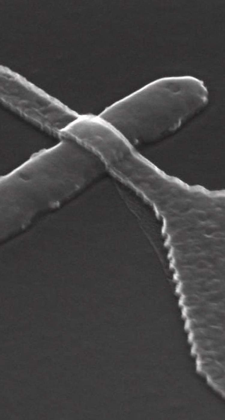
In the backend, there is progress in incorporating airgaps in high aspect-ratio metal lines to enable RC scaling.
In the realm of quantum computing, we work towards lowering charge noise in silicon spin qubit devices which is very promising for high fidelity qubit operation for quantum computing.
In the backend, there is progress in incorporating airgaps in high aspect-ratio metal lines to enable RC scaling.
As the data rates supported by optical IOs increase, the electric IC and the photonic IC are more closely integrated using co-packaged optics to reduce parasitics. We are developing new modules to making co-packaged optics a reality.
In the active memory program, we continue to improve the device performance and reliability of IGZO (indium-gallium-zinc-oxide) devices, which will play a key role in future scaled DRAM architectures. In our storage program, we keep on pushing the conventional gate-all-around 3D NAND Flash scaling roadmap for storage applications.


