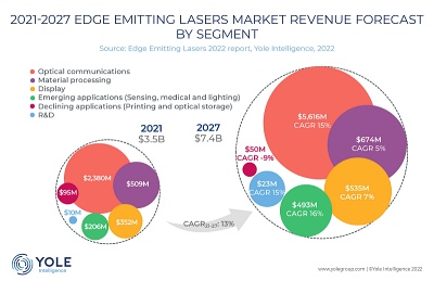
EELs used in optical communications will grow at a CAGR of 15% to be worth $5.6 billion in 2027 – representing 75% of the market.
The second-largest application area will be materials processing, with a CAGR of 5% to reach $674 million by 2027.
The growth areas, alongside new applications in sensing and displays, will more than offset the anticipated decline of printing and optical data storage applications, once the main applications for laser diodes.
That trend was highlighted by Epson’s recent decision to phase out laser printers, and Yole’s figures indicate that printing and storage applications will represent a market for EELs worth less than $50 million by 2027.
“The semiconductor laser landscape, and especially edge-emitting lasers, is highly fragmented,” says Yole. “Traditional applications cover industrial, telecommunication, scientific, and consumer markets. There are also many niche applications, including for the military and aerospace markets and spectroscopic analysis for the life science market.”
The variety of applications mean that device fabricators have to consider a broad set of technological parameters including wavelength, power output, spectral resolution, beam quality, and optical intensity for specific use cases.
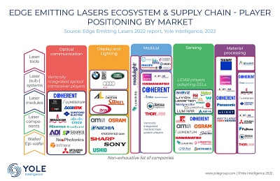
Those technological differences also result in each application area being defined by its own specific supply chain, leading to a highly fragmented and diversified industry.
“Understanding application requirements and evaluating laser parameters is, therefore, key to making the right investment decisions,” added Yole. “This is even more important as EEL prices vary widely depending on design and technical parameters.”
The company says that Fabry-Pérot devices are the most common EEL design in current use, with distributed Bragg reflector (DBR), external-cavity lasers (ECLs), distributed feedback (DFB) lasers, and quantum cascade lasers (QCLs) among the others that are used widely in different applications.
One emerging area could be indium phosphide (InP) EELs for depth sensing modules in smart phones. Because of a longer emission wavelength, such devices could be placed beneath an organic LED display and transmit through it.
Apple is known to be investigating the technology, as it would enable a larger display by reducing the size of the “notch” that houses an iPhone’s front-facing camera and sensor.
Another possibility for InP EELs is lidar, where more relaxed eye safely regulations at longer wavelengths allow greater power to be deployed, helping to improve signal-to-noise performance and achieve a longer sensing range.


