Such a ceremony is unusual and is being held, it is said, to emphasise that TSMC’s technology development and initial deployment takes place in Taiwan – at a time when the company has started building plants outside Taiwan.
Recently TSMC said that its investment in manufacturing facilities in the USA would rise to $40 billion from the initial $12 billion planned, and that it would build a 4nm plant in Arizona coming on-stream in 2024 and a 3nm Arizona fab coming on-stream in 2026.
The investment aims to deliver an Arizona-based capacity of 600,000 wafers a year of 4nm and 3nm chips.
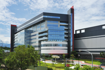
Tomorrow’s ceremony will take the form of a topping out event celebrating the installation of the final beam of the 3nm facility in the Southern Taiwan Science Park in Taiwan.
The 3nm process is finfet-based, as will be the upgrade to the process called N3E scheduled for introduction next year.
It is reported that TSMC is charging $20k for a 3nm wafer – a benefit of being the only company in volume production on 3nm.
Intel, which is trying to catch up with TSMC, plans to introduce a 3nm GAA process next year which could, possibly, match or beat TSMC’s N3E process for density and/or performance.
Samsung says it has been running 3nm GAA wafers since June, but reports say yield is below 20%.
TSMC plans to be on 2nm GAA, its first GAA process, in 2025, – the year Intel plans to be on its second generation GAA process called 18A.
.


