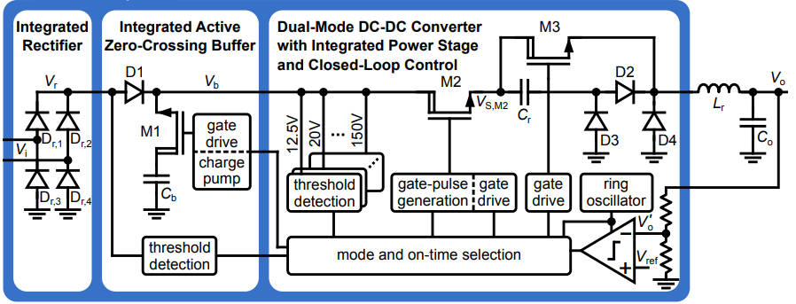
The only external components are the output inductor and capacitor, both low-voltage parts.
It can produce an adjustable 3.3 to 10Vdc from 15 to 325V ac or dc (a bridge is built-in) delivering up to 50mW, or 3oomW with one additional surface-mount capacitor.
Every half-cycle, the circuit works in three different modes.
From 12V to 150V on the internal dc rail (Vb in the diagram), transistor M3 is off and M2 operates the circuit as a constant on-time buck converter.
However, although the on-time is constant within the control loop, to balance conduction and switching losses for best efficiency, an open-loop circuit (threshold detection) reduces on-time in nine steps (360 – 68ns) as the input climbs from 12V to 150V. This happens in every cycle, both as voltage increases at the beginning of the mains cycle and towards the end as it decreases.
By the time Vd reaches 150V during each half-cycle, capacitive losses are dominating (and the on-time is getting a too short for reliable operation), so the IC automatically switches to resonant-mode operation, with M2 and M3 taking turns to resonate the output inductor with capacitor Cr (see diagram) using a combination of zero-voltage and zero-current switching.
Which ever mode it is in, operating frequency scales with frequency from ~1kHz at light load to ~2MHz at maximum power.
To get the output to ride through mains zero-crossing without a large reservoir capacitor, an on-chip capacitor (Cb) is charged to peak Vd through diode D1 and the parasitic diode of high-voltage transistor M1.
As the mains cycle drops towards 12V, a third operating mode is entered where, activated by its own threshold detector, M1 is turned on, dumping the Cb into Vb, causing Vb to briefly spike back up to the mains peak voltage. The bandwidth of the regulator is high, resulting in <200mV of disturbance in the output voltage during this large fast Vb transient.
On-die Cb is sufficient to ride through zero-crossing for loads up to 50mW. To boost this to 300mW, an external 0805 capacitor is needed: 12nF for 230Vrms operation, increasing to 47nF if the circuit has to work on 110V mains. Active die area is 12mm2 ignoring Cb and 16mm2 with it.
Power density is 458mW/cm3 and efficiency peaks at 73.7% (110Vin 10Vout) – although efficiency from 230V largely hovers around 50%.
As this is a non-isolated ac-dc converter, it is only proposed for applications that can be fully insulated and to not need external connections – such as wireless IoT sensor nodes.
ISSCC 2022 paper 14.2
A 110V/230V 0.3W offline chip-scale power supply with integrated active zero-crossing buffer and voltage-interval-based dual-mode control
The diagram above was copied from Paper 14.2 within the ISSCC 2022 Digest of papers
ISSCC 2022 is the 69th International Solid-State Circuits Conference, a conference which is arguably the world showcase for advances in on-chip circuit design and system-on-a-chip implementation. During the week-long conference, hundreds of selected and invited papers are presented, from the US, Asia and Europe.


