The company is fabricating GaN-on-Si HEMTs on a 200mm CMOS-compatible process, for a power factor correction (PFC) boost converter application.
Hard switching test Vds=600V Vgs=6V 100kHz
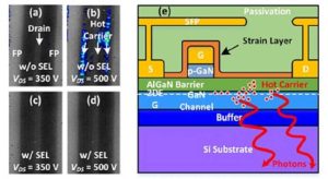
According to the company, it’s ‘stress enhance layer’ technology stabilises Rds(on) to <1.2x during a 1,000hr switching stress test, compared with an 18x dynamic Rds(on) degradation during the first three hours of stress without the stress enhance layer. ”

“By performing emission microscope to detect the electroluminescence of device in situ during switching stress, scientists at Innoscience have highlighted that the SEL suppressed the hot carrier injection, which is believed to contribute to the increase of the dynamic Rds(on) on samples without SEL technology”, according to the company.

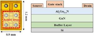
15V GaN HEMT in wafer-level chip-scale package, and its coree section
At the same conference, Innoscience is presenting a 15V GaN HEMT (right) with a 13.1mΩ·nC figure-of-merit, made on its 200mm GaN-on-Si platform.
“Although tremendous efforts have been made in low voltage GaN HEMT for consumer electronics, where power switches are typically below 40V, the wide adoption of low voltage GaN HEMT still faces huge challenge as compared with its silicon counterpart as the contact resistance or parasitic capacitance proportion rises up as dimensions shrink down, the threshold voltage Vth decreases and the risk of false turn-on increases, off-state leakage current increases and results in large quiescent loss and long-term static and dynamic instability,” said the company. “All these issues hinder the wide acceptance of low voltage GaN HEMT in volume constrained portable electronics.”
It is claiming “minimum parametric shift” (dynamic Ron and Vth) after 1,000 hours of stress with hard and soft-switching. The device was also tested in a half-bridge in a buck converter, achieving >80% efficiency at “tens of MHz”, said the company.
The ISPSD2022 programme of technical papers can be found here
Innoscience ‘on-line posters’ at ISPSD 2022:
- Evaluation of reliability and lifetime of 650-V GaN-on-Si power devices
fabricated on 200-mm CMOS-compatible process platform for high-density
power converter application - Dynamic Rdson and Vth free 15 V e-mode GaN HEMT delivering low FOM of
13.1 mΩ·nC and over 90% efficiency at 10MHz for buck converter


