Called 1ED332x, and branded ‘F3 Enhanced’, they come in 300mil wide DSO 16 packaging with 8mm creepage distance.
Operation is expected with devices between 600V and 2.3kV – abs max output supply for the output side of the chip is 40V.
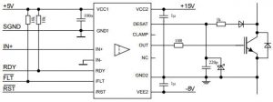
 Bipolar output-side supplies can be used to pull the gate negative (left).
The input-side chip inside can be directly connected to a standard
3.3 or 5V DSP or microcontroller, and dual inputs allow either logic polarity to be used.
Typical propagation delay is 85ns, and the company claims 15ns max IC-to-IC propagation delay matching.
“The tight propagation delay matching allows minimum deadtime improving system efficiency and decreasing harmonic distortion,” it said. “The driver family provides short-circuit clamping and active shutdown as well as an active Miller clamp.”
Isolation is though a coreless transformer, and safety certification is to UL 1577 with Viso at 6,840Vrms for 1s and 5,700Vrms for 60s. Insulation intended to be reinforced to VDE 0884-11 with Viorm = 1,767Vpeak (pending).
Application is expected in industrial drives, solar systems, electric vehicle charging, energy storage and commercial air conditioning.
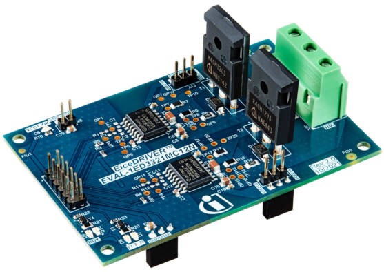
EVAL-1ED3321MC12N is the matching evaluation board (pictured).


